(China (Mainland))

Product Summary
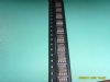
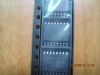
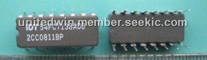
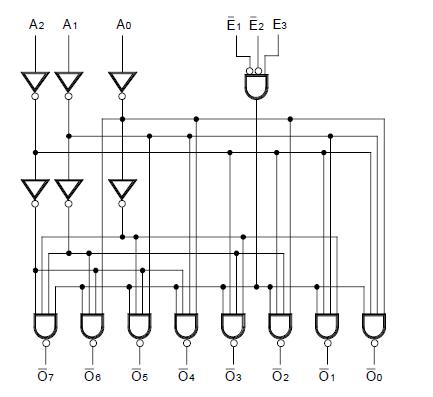
The IDT54FCT138ADB is a 1-of-8 decoder built using an advanced dual metal CMOS technology. The IDT54FCT138ADB accepts three binary weighted inputs (A0, A1, A2) and, when enabled, provide eight mutually exclusive active LOW outputs (O0 - O7). The IDT54FCT138ADB features three enable inputs, two active LOW (E1, E2) and one active HIGH (E3). All outputs will be HIGH unless E1 and E2 are LOW and E3 is HIGH. This multiple enable function allows easy parallel expansion of the device to a 1-of-32 (5 lines to 32 lines) decoder with just four IDT54FCT138ADB devices and one inverter.
Parametrics
IDT54FCT138ADB absolute maximum ratings: (1)Terminal voltage with respect to GND, VTERM: -0.5 to +7.0 V; (2)Terminal voltage with respect to GND, VTERM: -0.5 to VCC V; (3)Operating temperature, TA: 0 to +70℃ to -55 to +125℃; (4)Temperature under bias, TBIAS: -55 to +125℃ to -65 to +135℃; (5)Storage temperature, TSTG: -55 to +125℃ to -65 to +150℃; (6)Power dissipation, PT: 0.5W; (7)DC output current, IOUT: 120mA.
Features
IDT54FCT138ADB features: (1)IDT54/74FCT138A 35% faster than FAST; (2)Equivalent to FAST speeds output drive over full temperature and voltage supply extremes; (3)IOL = 48mA (commercial) and 32mA (military); (4)CMOS power levels (1mW typ. static); (5)TTL input and output level compatible; (6)CMOS output level compatible; (7)Substantially lower input current levels than FAST (5mA max.); (8)JEDEC standard pinout for DIP and LCC; (9)Product available in radiation tolerant and radiation enhanced versions; (10)Military product compliant to MIL-STD-883, Class B; (11)Standard military drawing # 5962-87654 is listed on this function.
Diagrams
 |
 IDT54 |
Other |
|
Data Sheet |
Negotiable |
|
||||
|
IDT54/74FCT646 |
Other |
|
Data Sheet |
Negotiable |
|
||||
|
IDT54/74FCT646A |
Other |
|
Data Sheet |
Negotiable |
|
||||
|
IDT54/74FCT646C |
Other |
|
Data Sheet |
Negotiable |
|
||||
|
IDT54/74FCT827A |
Other |
|
Data Sheet |
Negotiable |
|
||||
|
IDT54/74FCT827B |
Other |
|
Data Sheet |
Negotiable |
|
||||